Application Examples
Detlef Smilgies
In the final section we shall discuss a number of special cases
which
are important for the experimental application.
1) One layer
There are two possible situations: the layer has either a smaller or
a larger
d than the substrate. What kind of
signal do we expect in each case? It δ of
the
film is smaller than δ of the substrate
(e.g.
silicon film on a gold surface), we will first reach the critical angle
of the film starting from zero incidence. Beyond the critical angle the
wave will penetrate the film and reach the substrate which still
totally
reflects the incident wave. Hence there will be strong interference
fringes
between the critical angle of the film and the critical angles of the
substrate,
the so-salled Kiessig fringes (H. Kiessig, Ann. Phys. Leipzig 10, 769
(1931).).
In the other situation (Au on silicon), the reflectivity from the
film-substrate
interface is already quite low by the time the wave penetrates through
the the film and we will see only weak fringes in the tail of the
reflectivity
curve.
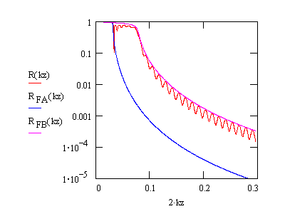
Low Z film on high Z substrate. The reflectivity curve (red)
features
strong oscillations between the critical angles of the two materials.
The
minima are related to excitation of a waveguide mode in the film (see
below).
Above the substrate critical angle regularly spaced oscillations, also
called Kiessig fringes, appear. The blue curve (film) and the magenta
curve
(substrate) show the respective Fresnel reflectivity.
|
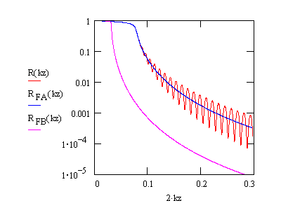
High-Z film on low-Z substrate. The reflectivity curve (red)
shows no
oscillations between the critical angles; moreover, the Kiessig
oscillations
only start gradually beyond the critical angle of the film. The blue
(film)
and magenta (substrate) curves show the Fresnel reflectivity.
|
The smallest layer spacing observable is given by the
signal-to-noise
of the experimental set-up. Typically 6 (rotating anode) to 8 orders
(synchrotron
radiation) of magnitude of the reflected intensity are detected. In the
latter case the limit of detection is around 10Å layer thickness.
This is enough to see a single monolayer of molecules, for instance
fatty
acids or lipids at the air-water interface or thiols (Self-Assembled
Monolayers)
on gold surfaces with a typical thickness between 15 and 30Å.
2) Two Layers: Waveguide Modes
If we make a special structure, for example Si:C:Si (bulk), the wave
can be trapped by total external reflection between
the Si substrate and the Si top layer and travel parallel to the
surface
in the C layer: We have made a wave guide for x-rays.
The wave guide will trap modes, if the thickness of the C layer
matches
n π/k'z , n=1,2,3,... - then we
have
the nodes of the trapped wave on the top- and bottom interface of the
wave
guide. The excitation of such a waveguide mode will show up as a sharp
dip in the reflected intensity - the dip will be the sharper and
shallower,
the less damping or losses the guided mode experiences. The wave guide
layer in the example below is 500Å thick and covered with a
50Å
top layer of the substrate material. Five resonances can be observed
between
the critical angles.
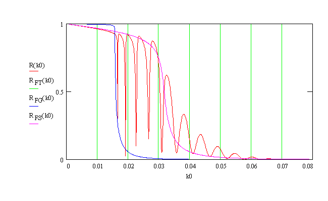
The blue and magenta lines indicate the Fresnel reflectivities of
the
guiding layer and the cladding layer, respectively.
Beyond the critical angle of the substrate, thickness oscillations
appear that can be used to characterize the waveguide structure.
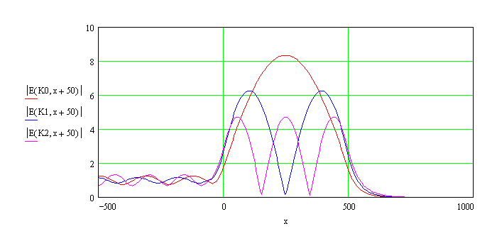
Wave amplitudes associated with the first three resonances TE0, TE1,
TE2. For the
0th order resonance (no node) the field is amplified by a factor of 8,
i.e. the energy density is 60 times higher than in the incident beam !
In the guided mode the electrical field is enhanced. Mike Bedzyk and
co-workers at CHESS have shown, how the enhanced field can be used to
detect
fluorescence from dopant atoms in the layer. In fact, if the
concentration
and spatial distribution of the dopant atoms is known well, it can be
used
to measure the electric field in turn. Not only the fluorescent yield
but
also diffuse scattering experiences such a resonant enhancement. This
effect
can be used to study defects, nano particles, or lateral density
variations
in the guiding layer.
Eventually the guided wave will travel to the edge of the substrate
or an uncoated part of the substrate and radiate into air. This guided
wave is coherent and very compressed in height. Wave guides have been
used
as microfocussing optical elements.
Actually even a single layer of lower electron density than the
substrate will give rise to wave guide modes between the critical
angles, as can be seen in the above example for the one-layer case.
Naturally the resonances are leakier in the one-layer mode, hence the
resonances broaden close to the substrate critical angle. Nontheless,
Jin Wang and coworkers have shown that the resonances can be used for
resonance-enhanced GISAXS, for which the TE0 mode is particularly
useful. Jin Wang and coworkers also showed that the
higher-order modes can be used for slicing the layer into different
active parts according to to the electric field strength, and thus
gaining more detatiled information about the distribution of materials
inside the film.
3) Multilayers
If a periodic structure of layers with different refractive indices
is prepared, we will get "Bragg reflection" at the corresponding angle.
The width of this Bragg peak depends on how many layers contribute to
the
scattering, i.e. the penetration depth. The angular width of the Bragg
peak is directly related to the energy-acceptance at fixed angle by
Bragg's
law. Thus a W:C multilayer accepts a bandwidth of 2-3% at 10 keV,
whereas
a Mo:B4C layers has a bandwidth around 1-1.5%. Another
advantage
of a Mo-based multilayer is that there are no absorption edges within
the
G-line energy range from 8 to 16 keV.
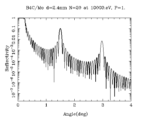
Multilayer reflectivity as calculated with the help of the CXRO web
site. In this example the top layer is B4C, the bottom layer
is Mo, with a thickness of 1/3 of the multilayer period of 24Å. A
total of 20 layers are used and ideal interfaces are assumed. The
G-line
multilayers will actually use 200 periods, so the diffraction peaks
will
be about 10 times sharper (the actual factor is determined by the x-ray
attenuation). In this case a reflectivity close to 100% can be achieved
for the first order multilayer peak. With a realistic interlayer
roughness
of 3-4Å we expect reflectivities of better than 50% based on some
first test pieces.
4) Free-standing layers
We can also use our formulism to study free-standing layers. Classic
examples are soap films or liquid crystal films that can be suspended
in
a frame and are pulled flat by the surface tension. Such films can be
as
thin as 100Å, i.e. cannot be analyzed with optical techniques.
From
such systems we can look at either the reflected or the transmitted
intensity.
For practical purposes the reflectivity yields the better information -
it
is much easier to measure a small signal on a small background than
measure
the small deviation in the high transmission of the incident x-ray
beam.
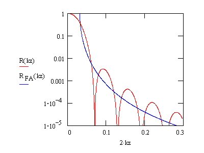
Reflectivity (red) of a freestanding 100Å film. For
comparison
the Fresnel reflectivity of the bulk
material is shown in blue.
|
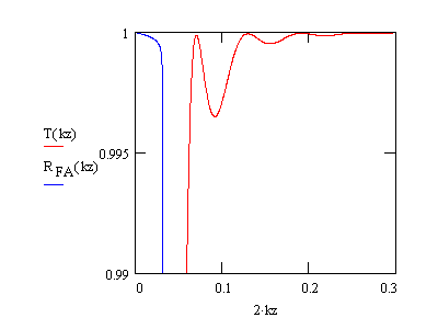
Transmissivity of the same 100Å film. The variations
within the
transmittivity amount to only fraction of 1%. The blue curve shows the
Fresnel reflectivity
and the critical angle of the bulk material.
|